This process was named after the prominent Polish scientist and subject of the Russian Empire, Jan Czochralski, who invented it back in 1915. The discovery happened by chance, although Czochralski’s interest in crystals, of course, was not accidental, because he studied geology very closely.
Application
Perhaps the most important area of application of this method is industry, especially heavy. In industry, it is still used for the artificial crystallization of metals and other substances, which cannot be achieved in any other way. In this regard, the method has proved its almost absolute lack of alternativeness and universality.
Silicon
Monocrystalline silicon - mono-Si. It has another name. Silicon grown by the Czochralski method - Cz-Si. That is, Czochralski silicon. This is the main material in the production of integrated circuits used in computers, televisions, mobile phones and all types of electronic equipment and semiconductor devices. Silicon crystals are also used in large quantities by the photovoltaic industry for the production of conventional mono-Si solar cells. An almost perfect crystalline structure gives the highest conversion efficiency of light into electricity for silicon.
Melting
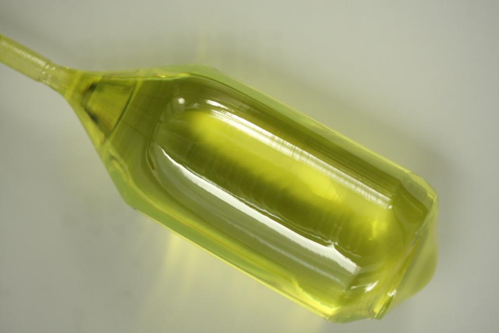
High-purity semiconductor silicon (only a few parts per million impurities) is melted in a crucible at 1425 ° C (2.597 ° F, 1.698 K), usually from quartz. Additive impurity atoms, such as boron or phosphorus, can be added to molten silicon in an exact amount for doping, thereby changing it to silicon type p or n with different electronic properties. A precisely oriented rod-seed crystal is immersed in molten silicon. The stem of the seed crystal slowly rises up and rotates simultaneously. Thanks to the precise control of temperature gradients, drawing speed and rotation speed, a large single-crystal cylindrical ingot can be extracted from the melt. Undesirable instabilities in the melt can be avoided by examining and visualizing temperature and velocity fields. This process is usually carried out in an inert atmosphere - such as argon, in an inert chamber - such as quartz.
Industrial Subtleties
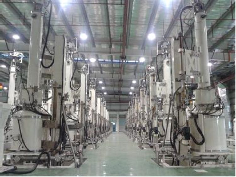
Due to the efficiency of the general characteristics of crystals, semiconductor industry uses crystals with standardized sizes. In the early days, their boules were smaller, only a few inches wide. With advanced technology, manufacturers of high-quality devices use plates with a diameter of 200 mm and 300 mm. The width is controlled by precise temperature control, rotation speed and speed of removal of the seed holder. The crystalline ingots from which these plates are cut can have a length of up to 2 meters, weighing several hundred kilograms. Large wafers can improve production efficiency, since more wafers can be made on each wafer, so a steady drive has increased the size of silicon wafers. The next step up, 450 mm, is currently planned to be introduced in 2018. Silicon wafers typically have a thickness of about 0.2-0.75 mm and can be polished to great flatness to create integrated circuits or texturing to create solar cells.
Heating
The process begins when the camera heats up to about 1500 degrees Celsius, melting silicon. When silicon is completely melted, a small seed crystal mounted on the end of the rotating shaft slowly lowers until it is below the surface of the molten silicon. The shaft rotates counterclockwise, and the crucible rotates clockwise. The rotating rod then stretches up very slowly - about 25 mm per hour in the manufacture of a ruby crystal - with the formation of an approximately cylindrical boule. The boule can be from one to two meters, depending on the amount of silicon in the crucible.
Electrical conductivity
The electrical characteristics of silicon are controlled by adding to it a material, such as phosphorus or boron, before it is melted. The added material is called dopant, and the process is called doping. This method is also used with non-silicon semiconductor materials such as gallium arsenide.
Features and Benefits
When silicon is grown according to the Czochralski method, the melt is contained in a crucible of silica. During growth, the crucible walls dissolve in the melt, and the resulting substance contains oxygen at a typical concentration of 1018 cm-3. Oxygen impurities can have beneficial or harmful effects. Carefully selected annealing conditions can lead to the formation of oxygen deposits. They affect the capture of unwanted transition metal impurities in a process known as gettering, improving the purity of the surrounding silicon. However, the formation of an oxygen precipitate in unintentional places can also destroy electrical structures. In addition, oxygen impurities can improve the mechanical strength of silicon wafers by immobilizing any dislocations that may be introduced during processing of the device. In the 1990s, it was experimentally shown that a high oxygen concentration is also useful for the radiation hardness of silicon particle detectors used in harsh radiation conditions (such as the LHC / HL-LHC CERN projects). Therefore, radiation detectors made of silicon grown by the Czochralski method are considered promising candidates for participation in many future experiments in high-energy physics. It was also shown that the presence of oxygen in silicon increases the capture of impurities in the process after implantation of annealing.
Reaction problems
However, oxygen impurities can react with boron in an illuminated environment. This leads to the formation of an electrically active boron-oxygen complex, which reduces the efficiency of the cells. The output of the module drops by about 3% during the first few hours of lighting.
The concentration of the impurity in the solid crystal resulting from the freezing of the volume can be obtained from consideration of the segregation coefficient.
Crystal growing
Crystal growth is a process in which an already existing crystal becomes larger as the number of molecules or ions in their positions in the crystal lattice increases, or the solution turns into a crystal, and further growth is processed. The Czochralski method is one of the forms of this process. A crystal is defined as atoms, molecules, or ions located in an ordered repeating sample, a crystal lattice that propagates in all three spatial dimensions. Thus, crystal growth differs from the growth of a liquid droplet in that during the growth of the molecule or ions must fall into the correct lattice positions so that an ordered crystal can grow. This is a very interesting process, which has presented science with many interesting discoveries such as the electronic formula of Germany.
The process of growing crystals is carried out thanks to special devices - flasks and lattices, in which the bulk of the process of crystallization of matter takes place. These devices in large numbers exist in almost every enterprise that works with metals, minerals and other similar substances. During the process of working with crystals in production, many important discoveries were made (for example, the electronic formula of germanium mentioned above).
Conclusion
The method to which this article is devoted played a large role in the history of modern industrial production. Thanks to him, people finally learned how to create full-fledged crystals of silicon and many other substances. First in the laboratory, and then on an industrial scale. The method of growing single crystals, discovered by the great Polish scientist, is still widely used today.