The transistor amplifier, despite its long history, remains a favorite subject of study for both beginners and venerable amateur radio enthusiasts. And that is understandable. It is an indispensable part of the most popular amateur radio devices: radios and amplifiers of low (sound) frequency. We will consider how the simplest low-frequency transistor amplifiers are built.
Amplifier frequency response
In any television or radio receiver, in every music center or sound amplifier you can find transistor sound amplifiers (low frequency - bass). The difference between transistor sound amplifiers and other types is their frequency response.
The sound amplifier on transistors has a uniform frequency response in the frequency band from 15 Hz to 20 kHz. This means that all input signals with a frequency within this range, the amplifier converts (amplifies) approximately the same. The figure below shows the ideal frequency response curve for a sound amplifier in the coordinates “amplifier gain Ku - input signal frequency”.
This curve is almost flat from 15 Hz to 20 kHz. This means that such an amplifier should be used specifically for input signals with frequencies between 15 Hz and 20 kHz. For input signals with frequencies above 20 kHz or below 15 Hz, the efficiency and quality of its operation are rapidly reduced.
The type of frequency response of the amplifier is determined by the radio electronic elements (ERE) of its circuit, and primarily by the transistors themselves. The sound amplifier on transistors is usually assembled on the so-called low- and mid-frequency transistors with a total passband of input signals from tens and hundreds of Hz to 30 kHz.
Class of work of the amplifier
As you know, depending on the degree of continuity of the flow of current over its period through a transistor amplifier stage (amplifier), the following classes of its operation are distinguished: "A", "B", "AB", "C", "D".
In the operation class, current "A" flows through the cascade for 100% of the input signal period. The cascade in this class is illustrated in the following figure.
In the class of operation of the amplifier stage "AB", more than 50% of the current flows through it, but less than 100% of the input signal period (see the figure below).
In the operation class of stage "B", exactly 50% of the input signal period flows through it, as the figure illustrates.
And finally, in the “C” cascade operation class, less than 50% of the input signal period flows through it.
Transistor woofer: distortion in the main classes of operation
In the working area, a Class A transistor amplifier has a low level of non-linear distortion. But if the signal has pulsed surges in voltage, leading to saturation of the transistors, then higher harmonics (up to the 11th) appear around each “standard” harmonic of the output signal. This causes the phenomenon of the so-called transistor, or metallic, sound.
If the low-frequency power amplifiers on transistors have unstabilized power, their output signals are modulated in amplitude near the frequency of the network. This leads to stiffness of sound on the left edge of the frequency response. Various methods of voltage stabilization make the design of the amplifier more complex.
The typical efficiency of a single-cycle class A amplifier does not exceed 20% due to the constantly open transistor and the continuous flow of the DC component of the current. A class A amplifier can be push-pull, the efficiency will increase slightly, but the half-waves of the signal will become more asymmetrical. Transferring a cascade from work class "A" to work class "AB" increases fourfold nonlinear distortion, although the efficiency of its circuit increases.
In amplifiers of the “AB” and “B” classes, distortions increase as the signal level decreases. Involuntarily, I want to cut such an amplifier louder to complete the feeling of power and dynamics of music, but often it helps a little.
Intermediate job classes
The class of work "A" has a variety - the class "A +". In this case, the low-voltage input transistors of the amplifier of this class operate in class "A", and the high-voltage output transistors of the amplifier, when they exceed the input signals of a certain level, go into classes "B" or "AB". Efficiency of such cascades is better than in pure class “A”, and non-linear distortion is less (up to 0.003%). However, their sound is also “metallic” due to the presence of higher harmonics in the output signal.
Amplifiers of another class - “AA”, the degree of non-linear distortion is even lower - about 0.0005%, but higher harmonics are also present.
Return to Class A transistor amplifier?
Today, many experts in the field of high-quality sound reproduction advocate a return to tube amplifiers, since the level of nonlinear distortion and higher harmonics introduced by them into the output signal is obviously lower than that of transistors. However, these advantages are largely offset by the need for a matching transformer between a high-resistance tube output stage and low-impedance speakers. However, a simple transistor amplifier can be made with a transformer output, which will be shown below.
There is also the point of view that only a hybrid tube-transistor amplifier can provide ultimate sound quality, all cascades of which are single-cycle, are not covered by negative feedbacks and work in class “A”. That is, such a power repeater is an amplifier on a single transistor. Its circuit can have the maximum achievable efficiency (in class "A") of not more than 50%. But neither the power nor the efficiency of the amplifier are indicators of the quality of sound reproduction. At the same time, the quality and linearity of the characteristics of all EREs in the circuit are of particular importance.
Since single-cycle schemes gain such a prospect, we consider below their possible options.
Single-ended amplifier on a single transistor
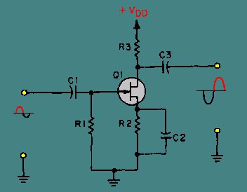
Its circuit, made with a common emitter and RC-connections for input and output signals for working in class "A", is shown in the figure below.
It shows the transistor Q1 of the npn structure. Its collector through the current-limiting resistor R3 is connected to the positive terminal + Vcc, and the emitter to -Vcc. The amplifier on the transistor of the pnp structure will have the same circuit, but the outputs of the power supply will change places.
C1 is an isolation capacitor by which the source of the variable input signal is separated from the source of constant voltage Vcc. At the same time, C1 does not interfere with the passage of the alternating input current through the base-emitter transistor Q1 junction. Resistors R1 and R2 together with the transition resistance "E - B" form a voltage divider Vcc to select the operating point of the transistor Q1 in static mode. Typical for this circuit is R2 = 1 kΩ, and the position of the operating point is Vcc / 2. R3 is a load resistor of the collector circuit and is used to create an alternating voltage of the output signal on the collector.
Suppose that Vcc = 20 V, R2 = 1 kOhm, and the current gain is h = 150. We select the voltage at the emitter Ve = 9 V, and take the voltage drop at the “E - B” junction equal to Vbe = 0.7 V. This value corresponds to the so-called silicon transistor. If we were considering an amplifier with germanium transistors, then the voltage drop at the open transition "E - B" would be equal to Vbe = 0.3 V.
Emitter current approximately equal to collector current
Ie = 9 V / 1 kOhm = 9 mA ≈ Ic.
Base current Ib = Ic / h = 9 mA / 150 = 60 μA.
Voltage drop across resistor R1
V (R1) = Vcc - Vb = Vcc - (Vbe + Ve) = 20 V - 9.7 V = 10.3 V,
R1 = V (R1) / Ib = 10.3 V / 60 μA = 172 kΩ.
C2 is needed to create a circuit for the passage of the alternating component of the emitter current (in fact, the collector current). If it did not exist, then the resistor R2 would strongly limit the variable component, so that the considered amplifier with a bipolar transistor would have a low current gain.
In our calculations, we assumed that Ic = Ib h, where Ib is the base current flowing into it from the emitter and arising when bias voltage is applied to the base. However, a leakage current from the Icb0 collector always flows through the base (both in the presence of bias and without it). Therefore, the real collector current is Ic = Ib h + Icb0 h, i.e. The leakage current in the OE circuit is amplified 150 times. If we were considering an amplifier based on germanium transistors, this circumstance would have to be taken into account in the calculations. The fact is that germanium transistors have a significant Icb0 of the order of several μA. In silicon, it is three orders of magnitude smaller (about several nA), so they are usually neglected in calculations.
Single-ended amplifier with an MOS transistor
Like any field-effect transistor amplifier, the circuit in question has its own analogue among bipolar transistor amplifiers . Therefore, we consider an analog of the previous scheme with a common emitter. It is made with a common source and RC-connections for input and output signals for work in class "A" and is shown in the figure below.
Here C1 is the same isolation capacitor by which the source of the variable input signal is separated from the constant voltage source Vdd. As is known, any field-effect transistor amplifier must have a gate potential of its MOS transistors below the potentials of their sources. In this circuit, the gate is grounded by a resistor R1, which, as a rule, has a large resistance (from 100 kΩ to 1 MΩ) so that it does not bypass the input signal. The current through R1 practically does not pass, so the gate potential in the absence of an input signal is equal to the ground potential. The potential of the source is higher than the potential of the earth due to the voltage drop across the resistor R2. Thus, the gate potential is lower than the source potential, which is necessary for the normal operation of Q1. Capacitor C2 and resistor R3 have the same purpose as in the previous circuit. Since this circuit has a common source, the input and output signals are phase shifted by 180 °.
Transformer Output Amplifier
The third one-stage simple transistor amplifier, shown in the figure below, is also made according to the scheme with a common emitter for working in class “A”, but it is connected to the low-impedance speaker via a matching transformer.
The primary winding of transformer T1 is the load of the collector circuit of transistor Q1 and develops an output signal. T1 transmits the output signal to the speaker and ensures matching of the output impedance of the transistor with a low (of the order of several ohms) speaker impedance.
The voltage divider of the collector power supply Vcc, assembled on resistors R1 and R3, provides the choice of the operating point of the transistor Q1 (supply bias voltage to its base). The purpose of the remaining elements of the amplifier is the same as in the previous schemes.
Push-pull sound amplifier
A push-pull low-frequency amplifier with two transistors splits the audio signal into two antiphase half-waves, each of which is amplified by its own transistor cascade. After performing such amplification, the half-waves are combined into a single harmonic signal, which is transmitted to the speaker system. Such a conversion of the LF signal (splitting and re-fusion), naturally, causes irreversible distortions in it, due to the difference in the frequency and dynamic properties of the two transistors of the circuit. These distortions reduce the sound quality at the amplifier output.
Push-pull amplifiers operating in class "A" do not reproduce complex sound signals well enough, since a constant current of increased magnitude continuously flows in their shoulders. This leads to asymmetry of the signal half-waves, phase distortion and, ultimately, to a loss of sound intelligibility. When heated, two powerful transistors double the signal distortion in the low and infra-low frequencies. But nevertheless, the main advantage of the push-pull circuit is its acceptable efficiency and increased output power.
The push-pull circuit of a transistor power amplifier is shown in the figure.
This is an amplifier for working in class "A", but class "AB", and even "B" can be used.
Transformerless transistor power amplifier
Transformers, despite the successes in their miniaturization, remain the most bulky, heavy and expensive EREs. Therefore, a way was found to eliminate the transformer from the push-pull circuit by performing it on two powerful complementary transistors of different types (npn and pnp). Most modern power amplifiers use this very principle and are designed to work in class “B”. The circuit of such a power amplifier is shown in the figure below.
Both of its transistors are connected according to the scheme with a common collector (emitter follower). Therefore, the circuit transfers the input voltage to the output without amplification. If there is no input signal, then both transistors are on the boundary of the on state, but at the same time they are off.
When a harmonic signal is applied to the input, its positive half-wave opens TR1, but puts the pnp transistor TR2 fully into cutoff mode. Thus, only a positive half-wave of amplified current flows through the load. The negative half-wave of the input signal opens only TR2 and locks TR1, so that the negative half-wave of the amplified current is supplied to the load. As a result, a full sinusoidal signal amplified in power (due to current gain) is allocated to the load.
Single Transistor Amplifier
To assimilate the above, we will assemble a simple amplifier on transistors with our own hands and see how it works.
As a load of a low-power transistor T of type BC107, we turn on headphones with a resistance of 2-3 kΩ, we apply bias voltage to the base from a high-resistance resistor R * of 1 MΩ, we disconnect an electrolytic capacitor C from 10 μF to 100 μF in the base circuit T. Feed the circuit we will be on the battery 4.5 V / 0.3 A.
If resistor R * is not connected, then there is neither base current Ib nor collector current Ic. If the resistor is connected, then the voltage at the base rises to 0.7 V and a current Ib = 4 μA flows through it. The current gain of the transistor is 250, which gives Ic = 250Ib = 1 mA.
Having assembled a simple amplifier on transistors with our own hands, we can now test it. Connect the headphones and place your finger on point 1 of the circuit. You will hear a noise. Your body perceives the radiation of the mains at a frequency of 50 Hz. The noise you hear from the headphones is this radiation, only amplified by a transistor. Let us explain this process in more detail. An AC voltage with a frequency of 50 Hz is connected to the base of the transistor through capacitor C. The voltage at the base is now equal to the sum of the DC bias voltage (approximately 0.7 V) coming from the resistor R * and the AC voltage "from the finger". As a result, the collector current receives a variable component with a frequency of 50 Hz. This alternating current is used to shift the speaker membrane back and forth with the same frequency, which means that we can hear a 50 Hz tone at the output.
Listening to a noise level of 50 Hz is not very interesting, so you can connect low-frequency signal sources (CD-player or microphone) to points 1 and 2 and hear amplified speech or music.