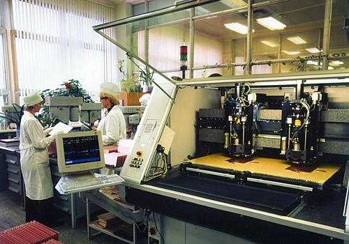
The printed circuit board is a structural element, which consists of a dielectric base and copper conductors, which are applied to the base in the form of metallized sections. It provides the connection of all electronic components of the circuit.
A printed circuit board has a number of advantages compared to bulk (mounted) mounting using cables and wires:
- high density installation of radio components and their connections, resulting in significantly reduced dimensions and weight of the product;
- obtaining conductors and shielding surfaces, as well as radioelements in a single technological cycle;
- stability, repeatability of such characteristics as capacitance, conductivity, inductance;
- high speed and noise immunity of circuits;
- resistance to mechanical and climatic influences;
- standardization and unification of technological and design solutions;
- reliability of nodes, blocks and the device itself as a whole;
- increased manufacturability as a result of complex automation of assembly work and control and regulatory actions;
- low complexity, material consumption and cost.
The printed circuit board also has disadvantages, but there are very few of them: limited maintainability and high complexity of adding design changes.
Elements of such boards include: dielectric base, metallized coating, which is a picture of printed conductors, pads; fixing and mounting holes.
The requirements that GOST imposes on these products
- Printed circuit boards should have a uniform dielectric base, which should be monolithic in structure, not contain internal bubbles, shells, foreign inclusions, cracks, chips, delaminations. However, single scratches, blotches of metal, traces of a single removal of a non-etched area, as well as a manifestation of a structure that does not change the electrical parameters of the product, does not reduce the allowable distance between the elements of the pattern, are allowed.
- The drawing is clear, with a smooth edge, without blisters, tears, delaminations, traces of the tool. Minor local etchings are allowed, but not more than five points per square decimeter, provided that the remaining width of the track will correspond to the minimum permissible; scratches up to six millimeters long and up to 25 microns deep.
To improve corrosion characteristics and increase solderability, the surface of the board is coated with an electrolytic composition, which should be continuous, without peeling, tearing and burning. The fixing and mounting holes must be located in accordance with the drawing. It is allowed to have deviations determined by the accuracy class of the board. In order to improve the reliability of soldering, a copper layer is sprayed onto all internal surfaces of the mounting holes, the thickness of which should be at least 25 microns. This process is called - plating holes.

What are PCB classes? By this concept is meant the accuracy classes of manufacturing boards, they are provided by GOST 23751-86. Depending on the density of the pattern, the printed circuit board has five accuracy classes, the choice of which is determined by the level of technical equipment of the enterprise. The first and second classes do not require high-precision equipment and are considered cheap in production. The fourth and fifth classes require special materials, specialized equipment, perfect cleanliness in production facilities, air conditioning, maintaining the temperature regime. Domestic enterprises massively produce printed circuit boards of the third accuracy class.