A differential amplifier (remote control) is used to amplify the difference between the two input signals. It can be considered as an analog circuit consisting of two inputs and one output.
Amplifiers used in various electrical and electronic circuits for generating signals and performing mathematical operations are called operational amplifiers (op amps). They are key components of an electronic analog computer. Their invention in the early 1940s led to the replacement of mechanical computing devices with quiet and fast electronics. Many analog computers relied on vacuum tubes sold by George Philbrick in 1952.
In 1963, Bob Widlar at Fairchild Semiconductor made op-amps on a single integrated circuit A702 - the very first monolithic operational amplifier IC.
Transistor amplifier circuit
The differential operational amplifier can be assembled according to the scheme as shown in the figure below, which consists of two transistors T1 and T2.
The remote control circuit has two inputs I1 and I2 and two outputs V1out and V2out. Input I1 is fed to the base terminal of transistor T1, input I2 is fed to the base terminal of transistor T2. The emitter outputs of transistor T1 and transistor T2 are connected to a common emitter resistor. Thus, the two input signals I1 and I2 will affect the outputs V1out and V2out. The circuit consists of two power supply voltages Vcc and Vee, but there is no grounding terminal. Even with a single supply voltage, the circuit can operate normally (similarly when using two supply voltages). Therefore, the opposite points of the positive voltage and the negative supply voltage are connected to ground.
Schematic diagram of the DT
The operation of the differential amplifier is shown in the diagram below.
If the input signal (I1) is supplied to the base of the transistor T1, then through the resistor connected to the transistor transistor T1, a positive voltage drop appears, which will be less. If the input signal (I1) is not supplied to the base of the transistor T1, then through the resistor connected to the transistor transistor T1, a positive voltage drop appears, which will be large.
We can say that the inverting output exiting through the collector terminal of transistor T1 is based on the input signal I1 supplied to the base terminal T1. If T1 is turned on using a positive value of I1, then the current passing through the emitter resistance increases when the emitter current and the collector current are almost equal. If the voltage drop across the emitter resistance increases, then the emitter of both transistors goes in a positive direction. If the emitter of transistor T2 is positive, then the base of T2 will be negative, and in this state the current will be less. And there will be less voltage drop across the resistor connected to the collector terminal of transistor T2.
Therefore, for this positive input collector, T2 will go in the positive direction. We can say that the non-inverting output that occurs at the collector terminal of transistor T2 is based on the input signal supplied to the base T1. The differential amplifier receives the output signal between the terminals of the collector of transistors T1 and T2. From the above circuit diagram, it is assumed that all the characteristics of the transistors T1 and T2 are identical, and if the base voltages Vb1 are equal to Vb2 (the base voltage of the transistor T1 is equal to the base voltage of the transistor T2), then the emitter currents of both transistors will be equal (Iem1 = Iem2).
Thus, the total emitter current will be equal to the sum of the emitter currents T1 (Iem1) and T2 (Iem2). Calculation of differential amplifier. Iem1 = Iem2 Ie = Iem1 + Iem2 Vev = Vb-Vb em I em = (Vb-Vb em) / Rem. Thus, the emitter current remains unchanged regardless of the value hfe of the transistors T1 and T2. If the resistances connected to the collector terminals T1 and T2 are equal, then their collector voltages are also equal.
A brief description of the operation of the operational amplifier
This amplifier (Op-amp, English version) may be ideal with infinite gain and bandwidth when used in Open-loop mode with a typical DC gain of more than 100,000 or 100 dB. The OA differential current amplifier has two inputs, one of which is inverted. The amplified difference of these inputs is output as voltage. The ideal operational amplifier has an infinitely high gain. It should express an infinity symbol with a new symbol. The operational amplifier operates either with double positive (+ V), or with corresponding negative (-V) power, or it can operate on one constant voltage supply.
Two basic laws related to OS
They consist in the fact that such an amplifier has an infinite input impedance (Z = ∞), which leads to the absence of current flowing into one of its two inputs and to a zero input bias voltage V1 = V2. The op amp also has zero output impedance (Z = 0). Optical amplifiers determine the difference between the voltage signals supplied to their two input terminals, and then multiply them by some predetermined gain (A). This gain (A) is often referred to as - Open Loop Coefficient. The op-amps can be connected in two main configurations - inverting and non-inverting.
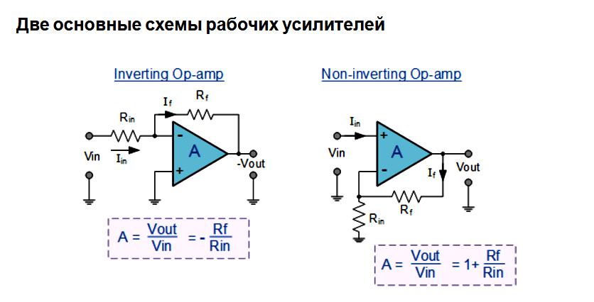
For negative feedback, if the feedback voltage is in antiphase at the input, the overall gain is reduced. For positive feedback, when the feedback voltage is in "phase", the input signal of the amplifier increases. By connecting the output back to the negative input connector, 100% feedback is achieved, as a result of which the voltage follower circuit (buffer) is obtained with a constant gain of 1 (Unity). Replacing the fixed feedback resistor (Rƒ) for the potentiometer, the circuit will have an adjustable gain.
Specifications
The main ones:
- The zero sequence input current (bias input current) is at rest, different currents can flow at two inputs. This in practice means that the voltage is distorted in the case of signal sources with high internal resistance, since the sources are subjected to different voltage levels.
- Input resistance can be measured against ground at the inputs, provided that the other input is grounded. The disadvantage here is sources with high internal resistance, which are partially loaded with input resistance.
- Input capacitance - capacitors parallel to the input resistors. They have a disturbing effect, especially at high frequencies, since capacitances create additional parallel input resistances, which depend on the frequency. For a differential amplifier, the principle of operation depends on this indicator.
- A low gain (increase in signal gain) indicates a gain that is obtained without feedback. It is determined with a load resistance of 2 kOhm and an output voltage fluctuation of ± 10 V. In practice, the indicated value of 200,000 has never been reached and is usually 10 times lower.
- The deviation coefficient of the supply voltage. With a change in the supply voltage of one volt, the bias changes by 0.3 μV. However, with a gain of 300 times, the error increases by 0.1 mV.
- Swing output voltage. An op-amp can never generate a full input voltage at its output. In any case, the maximum output voltage at an input voltage of ± 15 V will be significantly higher than ± 10 V. At normal loads, about ± 13 V and ideal - only 1 V below the supply voltage.
- Output impedance is the effective AC resistance at the output, only for output signals with low and offset output. Practically applicable only in borderline cases.
- Output short circuit current.
- Supply current with a unloaded operational amplifier, with a type of 1.7 mA.
- Performance - power losses, of course, in the unloaded operational amplifier caused by the supply current and depend on the operating voltage. A transistor differential amplifier needs a specific response time and degrades the hopping input signal. This applies to a load of 2 kΩ || 100 pF and the strengthening of "unity" (single gain).
- Rise rate to prevent uncontrolled span. If the output voltage changes to 10 V, the op-amp takes typically 5 μs. It becomes critical at high frequencies, as its output signal is greatly attenuated.
Boundary Application Conditions
The main ones:
- Supply voltage max. ± 18V. Most circuits operate at ± 15 V, therefore on the safe side.
- Maximum power loss (power dissipation) depends on the chassis version and the maximum allowable temperature. A simple 8-pin plastic casing can handle 310 mW, a 14-pin double-row casing can work about twice as much.
- Input voltages and differences can be in the range of -15 ... + 15 V. Solder. During soldering (soldering), the terminals are allowed to warm to 300 ° C for one minute. Soldering to the terminals is not performed simultaneously, but one after the other and only after the entire component is completely cooled.
- Short circuit on the output side. According to the manufacturer, the output short circuit can last indefinitely if all the boundary conditions are met.
- Limitation: the case temperature must not exceed 125 ° C, therefore the ambient temperature must not exceed 75 ° C
Differential amplifier using BJT
The principle of its operation is shown in the diagram below.
It is built using two matching transistors in a common emitter configuration, the emitters of which are connected to each other. A simple circuit capable of amplifying small signals between two inputs, while suppressing noise signals common to both inputs.
Bipolar Transistor Differential Amplifier (BJT) has a unique topology: two inputs and two outputs. Although you can use the signal from only one output, the difference between both outputs provides twice as much gain! And this improves common mode rejection (CMR) when the common mode signal is a noise source or DC bias from the previous step.
Transistor Computer Configuration
Based on input and output data input methods, differential amplifiers can have four different configurations, as shown below.
- Single-phase unbalanced output.
- Single input balanced output.
- Dual input unbalanced output.
- Dual input balanced output.
Schematic diagram of a DC amplifier
When developing analog building blocks (various types of preamplifiers, filters, etc.), it is important, along with the development of modern solutions for deep submicron technologies, to pay attention to new structural solutions of traditional amplification devices.
Differential DC amplifier (DUPT), its output voltage is proportional to the difference between the two input voltages. This can be represented in the form of an equation as follows: V out = A * ((Vin +) - (Vin-)), where A = gain.
Practical use
In practical circuits, the remote control is used to amplify: pulses over long wires, sound, radio frequencies, control of motors and servomotors, electrocardiograms, information on magnetic drives.
disadvantages
A differential amplifier has several disadvantages that somewhat limit its use in electronics:
- A low input resistance, depending on the resistor, for example, with a weak signal from a thermocouple - remote control will give an erroneous measurement result.
- A hardly adjustable gain, which will require a change in the value of two resistors, which is practically difficult to implement, and introducing additional elements (potentiometers or multiplexers) into the circuit will unnecessarily complicate the circuit.